Who wins in semiconductor design
SNPS +6/10 | CDNS +5/10
Takeaway: Chip design captures more durable value than chip manufacturing, and within design, the EDA "toll booth": Synopsys, Cadence, and Siemens EDA, controlling ~85% of the the market is the lowest-risk way to own the AI semiconductor buildout. Every company from Nvidia to a hyperscaler building its own silicon, still license EDA software to produce a chip. Between the two investable names, Cadence's stronger execution and margins are against Synopsys's larger scale and bolder (if debt-funded) bet on Ansys becoming a second growth engine.
Research series: This article maps who captures value in Semiconductor design, continuing on earlier research: Synopsys, Inc. (SNPS)

Total Semiconductor Market
The headline number moved dramatically recently. WSTS (World Semiconductor Trade Statistics), the industry’s independent data body, forecast in its Autumn 2025 update that the global semiconductor market would reach $975B in 2026, ~25% YoY. By Spring 2026 update, WSTS revised that figure to $1.51T, a 90% YoY increase, driven by memory.
HBM-linked memory demand is forecast to surge ~250% YoY, crossing $800B. A forecast nearly doubling within a few months is a measure of how fast this cycle is still accelerating.
The Design Market — Narrow vs. Broad
Two legitimate but very different “design market” figures circulate:
Narrow definition (EDA tools + design services + IP licensing): $18-21B for 2026, growing to $24-38B by 2030s (CAGR 7.8-11.3% across sources).
Broad definition (all fabless revenue, the total value of chips designed by companies that don’t own fabs): $228-468B range for 2025-2026 depending on methodology, growing at 6-8.5% CAGR.
Six Trends That Matter for Investors
1. AI Disruption
AI is simultaneously EDA’s tailwind and a threat to the category’s business model.
On July 17, 2026, both Synopsys and Cadence fell 9-10% after Moonshot AI’s Kimi K3 model reportedly designed a functional chip autonomously in 48 hours, a fear that AI could eventually replace design software, not just accelerate demand for it. The counter-context: the demo chip was built on a 45-nanometer process, described as “roughly 4 generations behind”, and why several analysts (BNP Paribas, Bloomberg) called the selloff overdone.
2. Agentic EDA Workflows
Synopsys, Cadence and Siemens EDA, are building AI agents that run chip verification, thermal simulation, and debug work autonomously. Vendor-reported: Synopsys’ Nvidia-built verification agent runs up to 50x faster while finding 20% more errors; a separate Microsoft-built debug-closure workflow showed a 25-40% reduction in cycle time.
3. Multiphysics Expansion
Both Synopsys and Cadence are moving beyond pure chip logic into physical simulation: heat, power delivery, and electromagnetic interference between densely packed components, via M&A.
Synopsys acquired Ansys, for $34.9B, closed July 17, 2025. Cadence acquired BETA CAE for $1.24B (closed May 2024), followed by Hexagon’s Design & Engineering (including MSC Software) for $3.1B (closed February 2026).
4. Chiplet Economy
Market size: $51.94 billion in 2025 (counting a whole of GPU or AI ASIC), growing at a 24.8% CAGR through 2033.
The driver: monolithic chip designs are hitting reticle size limits (the physical maximum size a single piece of silicon can be manufactured at), and a complete 3-nanometer tape-out, covering EDA licenses, IP fees, mask sets, prototyping, and verification, now runs $300-500 million, with mask sets alone costing $10-20 million.
A “monolithic” chip is one built as a single, continuous piece of silicon (the processing cores, memory controllers, I/O) etched onto one slab, rather than assembled from multiple smaller pieces.
The “reticle” is a manufacturing limit: it’s the mask a chipmaker’s lithography equipment projects onto a silicon wafer to etch a chip’s pattern, and that equipment can only expose a fixed maximum area in a single pass — roughly 26mm × 33mm, an industry-standard ceiling that hasn’t meaningfully changed in years.
A monolithic chip cannot be larger than what the reticle can expose in one shot. As AI chips demand more and more transistors packed in to boost performance, designers are running into this ceiling: you cannot make one continuous piece of silicon bigger than the equipment allows, no matter how much a customer is willing to pay for more compute.
Chiplets solve this. Instead of one monolithic chip, you build several smaller pieces separately, each within the reticle limit, and then connect them inside a single package, so they function as one larger, more powerful chip. This is the reason chiplets are becoming necessary: it’s the only way to keep scaling up total transistor count once you’ve hit the size limit a single piece of silicon can physically be.
A “tape-out” is the final step of sending a finished chip design to the factory for manufacturing. At the most advanced node (transistors are 3-nanometer apart), getting to that point costs $300-500M, including:
- EDA licenses, the design software
- IP fees, license for pre-built components rather than designing everything from scratch
- Mask sets, the stencils burned into the reticle to etch the pattern onto silicon, at $10-20 million
- Prototyping and verification: building and testing early versions before committing to production
If you’re already paying $300-500M to design and manufacture one advanced chip, and that chip is now hitting a size ceiling that caps how much performance you can pack into it, chiplets become the only way to keep scaling and to manage that enormous cost more sensibly. You can mix, for example, an expensive 3nm compute die (where the performance matters most) with a cheaper, older 7nm die for less performance-critical parts like I/O, rather than paying the 3nm cost for the entire chip. That’s the economic logic behind the shift to chiplets, not only the manufacturing limit.
5. RISC-V and the Open-Architecture Shift
RISC-V (“risk-five”) and the Open-Architecture Shift are a fundamental transition in how microprocessors are designed, licensed, and built.
- RISC (Reduced Instruction Set Computer): A processor design that uses a simplified, highly streamlined set of instructions. By keeping instructions basic, the hardware can execute commands much faster and with better energy efficiency. (“V” is the fifth generation of RISC design).
- Open-Architecture Shift: anyone can access the RISC-V specification, design a compatible chip, and manufacture it without paying licensing fees
A small but rapidly growing market, with dispersion across estimates: $2.49B (2025) to $10.77B (2030) at a 34% CAGR; a more conservative model shows $1.53B (2025) to $5B (2035) at 12.6% CAGR.
RISC-V remains tiny next to incumbent’s Arm Holdings 99% smartphone-market share, but the underlying driver is economic: Arm charges a 2-3% royalty on every chip; RISC-V is free and open-source, and geopolitical pressure (China’s push for chip self-sufficiency) plus automotive-sector cost pressure are accelerating adoption despite the small current base.
6. Node certification as the moat
Foundry certifications (TSMC’s A14 and N2P (September 2026), Samsung’s 2nm nodes, Intel’s 14A) matter because both major EDA vendors get certified on the same nodes at the same foundries.
This confirms the moat protects the EDA oligopoly as a whole, not one firm over another: a chip designer switching EDA vendors mid-design means years of work (Design flows, IP libraries, Trained engineers).
Competitive Landscape
Tier 1: EDA & Core IP — The Toll Booth
Key players: Synopsys, Cadence, Siemens EDA, Arm.
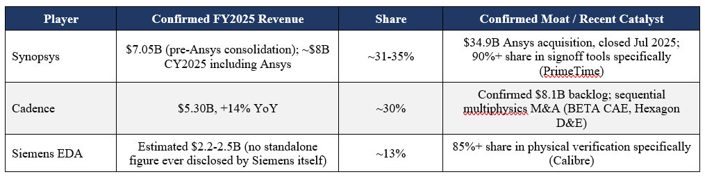
Combined Big-3 revenue: approximately $16 billion, tiny relative to the $228-468B broad fabless market these three companies’ tools make possible. Synopsys and Cadence have a combined 70% share (per Cadence’s SEC 10-K), rising to 83-85% once Siemens EDA is included.
Synopsys (SNPS)
Strengths: Larger scale ($9.42B vs. $5.84B revenue); expanded TAM via Ansys ($18-19B → $31B); real organic core growth (EDA +8.5% YoY).
Weaknesses: $10B debt from the Ansys deal; lower margins (72.4% gross, 11.4% net) than Cadence, diluted by Ansys’s lower-margin business; China revenue fell 22% in FY25 as export curbs pushed customers to local EDA alternatives; trails Cadence in hardware verification (ZeBu/HAPS vs. Palladium).
Cadence (CDNS)
Strengths: Stronger execution of the two (4/4 beat-and-raise); highest margins in the pair (88.5% gross, 23.6% net); leads in hardware verification; record $8.1B backlog; smaller, sequential M&A (BETA CAE, Hexagon D&E) carries lower integration risk than one large bet; actively pushing into Intel, “historically a Synopsys stronghold.”
Weaknesses: Weakest FCF yield in its own peer set (2.0% vs. 4.4% average); highest capex-to-revenue (3.0%); rich valuation (PEG 3.52) without a clear organic-growth edge to justify it.
Tier 2: Merchant Fabless Giants and Custom ASIC Specialists
Key players: Nvidia, AMD, Qualcomm, Broadcom, Marvell.
These companies design their chips in-house, but they don’t own or operate a “fab” (a fabrication plant that manufactures silicon wafers). Once the design is finished, they send it (almost always) TSMC to manufacture it.
Building and running a leading-edge fab costs tens of billions of dollars and takes years to set up. TSMC’s scale is the reason virtually no company tries to do both design and manufacturing. Intel is the major exception, and even Intel now manufactures for outside customers, too. By staying fabless, Nvidia, AMD, Qualcomm, Broadcom, and Marvell can focus their capital on chip design and software, where the margins are higher, without the fixed cost of owning a fab.
Where the “Custom ASIC” names (Broadcom, Marvell) differ
Broadcom and Marvell’s design work is partly co-designed with the hyperscaler customer, rather than fully independent like Nvidia’s GPU architecture. When Broadcom builds a custom chip for Google’s TPU program, Google specifies requirements and works alongside Broadcom’s engineers, but Broadcom still does the in-house EDA-tool-based design work (using Synopsys’s or Cadence’s software) and sends the finished design to TSMC for manufacturing. They’re fabless, too, just with a named customer involved in shaping what gets designed.
Broadcom and Marvell are co-designing custom AI accelerators (TPUs, Trainium-class chips) for hyperscalers, capturing multi-year contracts without taking on the product risk as a merchant GPU seller.
Tier 3: Hyperscaler In-House Design and Pure-Play Connectivity
Key players: Google (TPU), Amazon (Inferentia/Graviton), Meta (MTIA), Microsoft (Maia) on one side; Astera Labs (ALAB) and Rambus (RMBS) on the other.
The hyperscaler in-house units eliminate merchant-chipmaker margins entirely, but carry weaknesses: development cycles of 3+ years per generation, and continued reliance on third-party design partners (the Tier 1 and Tier 2 names above) for implementation. None of them design chips fully in-house without EDA tools or ASIC design-service partners.
Astera Labs is Nasdaq-100 component, $852.5M in 2025 revenue and $219.1M in net income. Its products (Aries, Taurus, Leo) address PCIe, Ethernet, and CXL connectivity, with one source citing its chips shipping in over 80% of AI servers.
What to Invest In
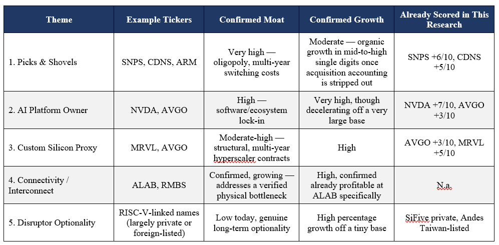
The table shows several real themes, with independent verification (rows 1-3) versus directionally promising but unverified (row 4) and inaccessible (row 5).
The takeaway
The EDA oligopoly is the lowest-volatility, highest-moat way to own this theme: whether Nvidia wins, a hyperscaler builds its own chip, or a new AI-silicon startup emerges, everyone of must license EDA software and pay IP royalties to design working silicon. Pricing power sits with the toll-booth operators, not the traffic.
The clearest risk worth flagging: the thesis assumes continued AI-driven demand.
Deloitte’s 2026 outlook states: the industry has “placed all its eggs in the AI basket,” and firms should plan for scenarios where that demand slows or reverses. The Americas region, in WSTS’s Spring 2026 data, is forecast to grow 112% in a year. A striking number, but one that is priced for a continuation of the current cycle, not a cushion against its interruption.
This article synthesizes fundamental data, company filings, and current public reporting — SEC filings, earnings call transcripts, WSTS industry data, and sell-side coverage — gathered via web research, alongside prior findings from research on SNPS, CDNS, NVDA, and AVGO. It is for information only and is not investment advice.